
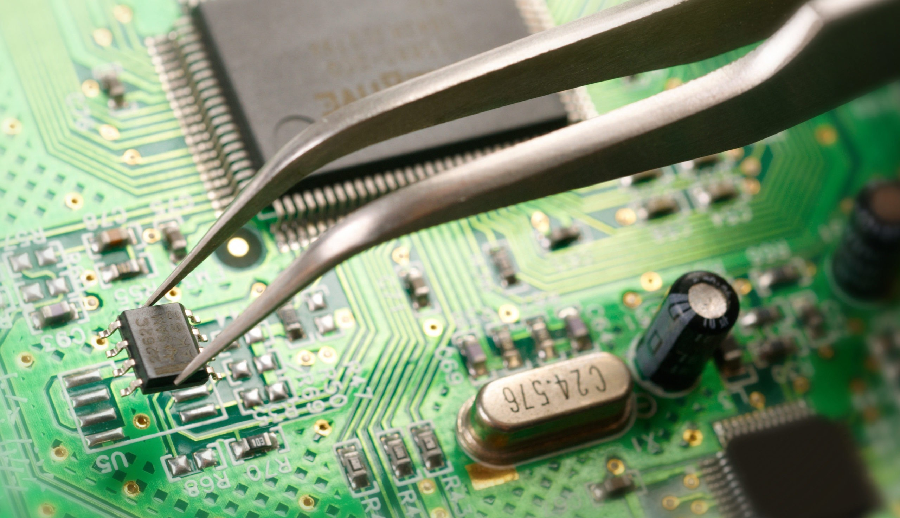
Take apart any electronic device, and you’re guaranteed to find a printed circuit board inside. This board allows the integration of multiple components that work hand-in-hand to achieve a multitude of functions — much like how your body’s internal organs are linked through nerves, blood vessels, and other structures. Wouldn’t it be interesting to find out how such clever mechanisms are achieved? Here’s a quick rundown of the basic printed circuit board manufacturing process.
Step 1: Schematic Design
Also known as the schematic diagram, this provides a representation of all the various component that will go on the PCB. Each component has its own unique identifying symbol. You’ll need to have a clear idea of what should go into your board before you can start designing. Once that’s taken care of, you can now use CAD software to map out the board’s blueprint. A trace width calculator will also come in handy when outlining the inner and outer layers.
Step 2: Review
Industry standards call for a thorough review of the schematic diagram to rule out potential errors/flaws. Engineers will usually check for incorrect structures and missing components. There are also software tools that can simulate the board’s function to ensure it’ll work as intended.
Step 3: Printing the Design
This is done using a special device known as a plotter printer, which makes a film outlining the board’s layers and details. The inner layer is depicted using two colors:
- Black for the circuits and copper traces
- Clear for the fiberglass base and other non-conductive areas
This color scheme is reversed for the board’s outer layers: Clear ink shows copper pathways, while black depicts the areas where copper will be removed. Also, each layer and the corresponding solder mask (protective coating) will require its own film. This equates to a total of 4 sheets for a simple dual-layer PCB man.
Once the films have been printed, they’re stacked up and a hole gets punched through them. This is known as a registration hole, and it acts as a guide for aligning the films during manufacture.
Step 4: Printing the Inner Layer on Copper
This is where the actual manufacture begins. The design is transferred onto a laminate board, after which copper is pre-bonded on both sides. Once the copper is etched to achieve the design as per the blueprint, the laminate board is covered using a photo-sensitive film known as the resist.
Step 5: Etching
It’s often necessary to rid the inner layer of excess copper prior to fabrication. Here, the board is exposed to a chemical that strips the unwanted areas; a protective layer is applied elsewhere to keep the copper lines clean.
Step 6: Alignment & Inspection
The board’s inner and outer layers are aligned by driving a pin down the registration hole. An optical inspection device then performs one final checks to ensure there are no defects. This is confirmed by comparing the board with the original design.
Step 7: Lamination & Bonding
The defect-free layers can now be fused to create a working PCB. The two are first laid onto an alignment basin along with several other accompanying layers. This stack is then transferred to a laminate press which applies pressure and heat to achieve bonding. Once this is done, the printed board can now be pulled out for the finishing process; this varies depending on what kind of PCB is being manufactured.


Comments